Speedy TT - English Version: Unterschied zwischen den Versionen
Gaga (Diskussion | Beiträge) |
Gaga (Diskussion | Beiträge) |
||
| Zeile 12: | Zeile 12: | ||
<small>''Abb2: PGA-Speedy Rev. 1v0''</small> | <small>''Abb2: PGA-Speedy Rev. 1v0''</small> | ||
[[Bild:Abb03_SMD- | [[Bild:Abb03_SMD-Speedy_1v0.JPG|400px]] | ||
<small>''Abb3: SMD-Speedy''</small> | <small>''Abb3: SMD-Speedy Rev. 1v0''</small> | ||
Version vom 23. Januar 2022, 22:30 Uhr
General
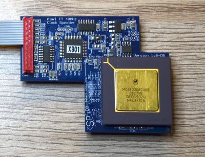
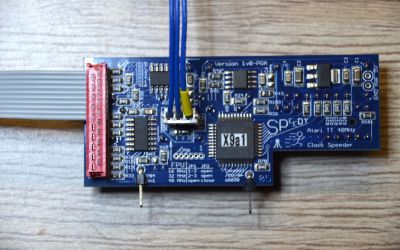
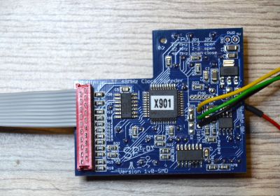
The Speedy TT is a small PCB board, which increase the clock speed of the processor (CPU) of an Atari TT. Speedy is available in three different PCBs, depending on your type of mainboard.
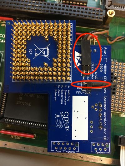
Abb1: Daughterboard Speedy Rev. 1v0
Abb2: PGA-Speedy Rev. 1v0
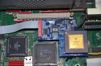
Abb3: SMD-Speedy Rev. 1v0
To decide, which type of Speed you need, please open your TT and have a look to your mainboard. Please remark, that the backside with connectors like monitor sub D connector, ACSI connector and so on is back, frontside is in front of you.
| Type of Mainboard | Identifying your Mainboard | Sort of Speedy |
|---|---|---|
| Daughterboard TT | Processor (PGA-Type) inside of an small PCB (Daughterboard) which is socket inside of the mainboard, Daughterboard is placed under the TT-RAM-Expansion-Port | Daughterboard-Speedy (short form: DB-Speedy) |
| PGA TT | Processor (PGA-Type) is directly socket inside of the mainboard, Processor is placed also close to the TT-RAM-Expansion-Port | Speedy for TT with PGA CPU (short form: PGA-Speedy) |
| SMD TT | Processor (SMD-Type) is soldered directly on your mainboard, Processor is placed under the ST-RAM-Expansions-Slot | Speedy for TT with SMD CPU (short form: SMD-Speedy) |
First of all: Please be note, that the installation of Speedy needs really advanced skills of soldering!
If you have a novice skill, please ask a competence person for help!
- Speedy allows you to speed up your CPU of your Atari TT up to 48 MHz.
- You can speed up your coprocessor (MC68882) of your Atari up to 48 MHz.
- If the increasing of speed doesn’t work inside of your TT, you don’t have to rework all steps! Speedy gives you the item to let them inside of your TT with normal speed.
- You could increase the access to your Alternate-RAM, if you bought the new STORM TT Rev. G. If you have an older STORM TT Revision, please make a request to your Thunderstorm Team to change the STORM TT to the newest Revision.
Technical Details
The data bus inside of all TT is depending of a 16 MHz bus speed. Atari decided short time for delivery of the first Atari-TTs to speed them up to 32 MHz. That means, that the CPU is clocked with a 32 MHz clock and the bus still driven by 16 MHz. The matching of these two clock cycles realized with two PAL/GALs (U111 and U112) and four 74F74 (U113 up to U116) inside of all TTs. In this explanation we say to this six ICs: “state machine”. The designation of these parts is in all sort of TTs the same one.
By the way: The daughterboard TT is the oldest version of mainboard. There you can see, that the TT was designed only for 16 MHz bus clock speed and 16 MHz processor clock speed. To increase the clock speed of the processor Atari made a PCB which handle this. This is the daughterboard. ☺ And the six ICs (U111 – U116) placed onto the daughterboard! The next generation of TTs is the “PGA version”. Same state machine, but now the state machine and processor are placed onto the mainboard. To reduce costs, inside the newest and latest version of TTs, Atari replace the PGA CPU at the mainboard with a SMD CPU.
Speedy replace the old state machine (remember: U111 – U116) and establish a new once, which allows us together with a PLL circuit to increase the processor speed at triple bus speed (3 x 16 MHz = 48 MHz).
To implement Speedy inside of your TT it is necessary to unsolder the old state machine. Means you have to unsold the six ICs U111 up to U116!
Another item in this case is, that the /BG (Bus Grant) signal inside of the Atari TT designed for a 16 MHz clock bus transfer. The timing match also, if the processor get an increased clock speed of 32 MHz.
Above 32 MHz this timing doesn’t matched together. The /BG signal from the CPU is to quick to recognized at the mainboard. The activation of this signal could get get lost between processor and mainboard. It’s incessant to split the /BG signal and loop it through the Speedy PCB. Speedy adapt the correct timing of the /BG signal, if the CPU is driven with 48 MHz clock speed. To split the /BG signal and to inject the new /BG signal into the mainboard is a second part, what we shall to do.
Depending of your Type of mainboard this means more or less work. If you have a daughterboard TT, it’s quite simple, because these six ICs are on the daughterboard! If you have a PGA or SMD version, it’s hard work!
Additionally, Speedy needs the both clocks (16 MHz and 32 MHz) of the mainboard. Both are easily available at the Jumper W101. W101 normally get the opportunity to switch the clock speed of the coprocessor. We use this jumper W101 to get these both clocks for Speedy. We connect all three pins of W101 to Speedy. The advantage now is, that we could offer the coprocessor 16 MHz, 32 MHz and also 48 MHz, depending which clock speed will accept from the coprocessor.
The procedure to prepare your TT is in all cases technical the same! The steps could look a bit different.
We will start the description for the SMD-TT. If you have another type of TT, please choose the chapter of your type of TT.
Open your TT and take the mainboard out of the case. Please be note of all additional part inside of your TT. Please make you some notes or pictures, which give you a good way to reassemble after all your TT in right order.
Conversion of a SMD TT
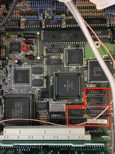
Your TT mainboard looks like the next picture. On the next picture you can see the six ICs which you have to unsolder.
Abb4: Mainboard SMD TT with marked ICs
Depending of your Revision of mainboard, you have to remove the clock patch of the processor clock. Atari did some clock patches inside some TT’s to optimize the clock trace of the processor.
- First type is, “no clock patch”. Easy: Only removing the six ICs is necessary.
no picture
- Second type of patch is a cable connected from U110 Pin 1 to resistor (R888):
Picture missed:
Abb.5: Second type of patch
- Third type of patch is a cable connected from R997 to U210 (74AC244) Pin 17 and a second cable connected from U210 Pin 3 to resistor (R888):
Abb6a-b: third type of patch
In case of the both last patches you remove all cables and replace the resistor R888 (10 Ohm) onto of the marked place at the mainboard without the cables.
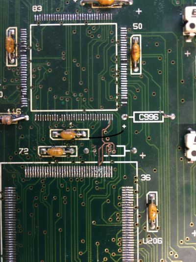
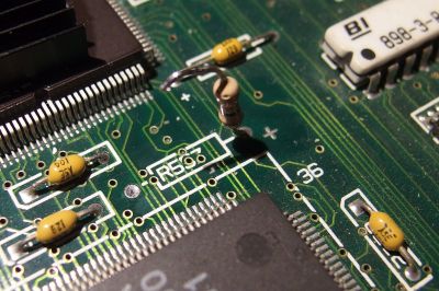
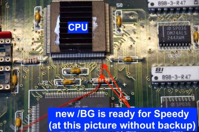
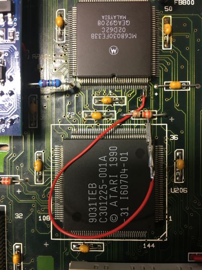
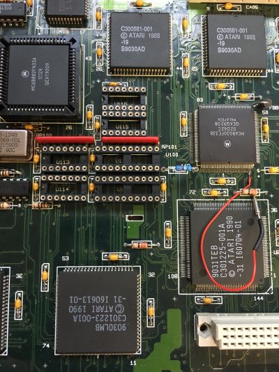
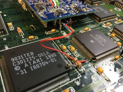
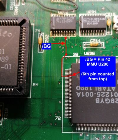
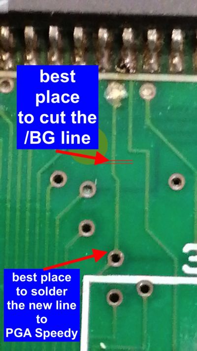
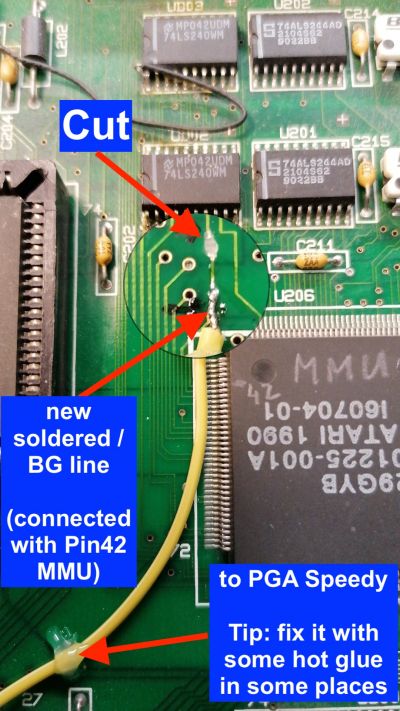
Next step is, to split the /BG signal coming from the CPU. We cut through the signal line onto the mainboard close to the CPU. The next picture shows a good place to divide the signal line of /BG signal.
Abb7a-d: CPU of SMD TT with divided /BG signal
/BG signal coming from the CPU get a small cable, which shall connect to Speedy. To fall back in the old situation, it is useful to install also a female socket pin on the opposite side of /BG signal. There you have every time the opportunity to jumper the /BG signal in old situation.
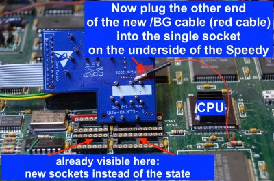
Connect the /BG signal from CPU into the free female socket pin under the Speedy PCB. Additional information: The new /BG signal from Speedy goes via U112 Pin 11 into the mainboard. There is nothing to do.
Abb8: Speedy with female socket under the PCB for injecting the /BG signal from the CPU
Be sure that all your changes matched with the next picture.
Abb9:SMD TT Mainboard with all changes, ready to install SMD-Speedy
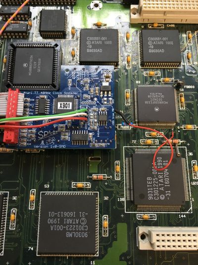
Abb10: SMD TT Mainboard with SMD-Speedy
After all, put Speedy on top of the sockets of U111 up to U116. Please be careful and check that all pins fit correctly into the right socket pins.
Put the small connector to all three pins of W101. The red cable is connected to Pin 1 of W101.
Conversion of a PGA TT
Your TT mainboard looks like the next picture. On the next picture you can see the six ICs which you have to unsolder.
Picture missed:
Abb. 11 Mainboard PGA TT with marked ICs
Next step is, to split the /BG signal coming from the CPU. The cut through of the /BG signal is into the PGA TT another one like in the SMD TT! This is be dept in case, that the place, where we can easily divide the /BG signal inside of the PGA TT is another place like into the SMD TT.
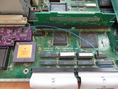
In the PGA TT the /BG signal line connect in normal way to Pin 11 of U112. So, the /BG signal of the CPU inject the Speedy at this pin. The new /BG signal for the mainboard connected at the female socket pin onto the Speedy. Over a small cable we connect this new signal into the mainboard at the place, shows in the next 3 pictures.
Abb12a-c: CPU of PGA TT with divided BG signal
To fall back in the old situation, you put the cable into Pin 11 of U112.
Picture missed:
Abb.13: PGA Speedy with female socket onto the PCB for injecting the /BG signal from the mainboard.
After all, put Speedy on top of the sockets of U111 up to U116. Please be careful and check that all pins fit correctly into the right socket pins.
Put the small connector to all three pins of W101. The red cable is connected to Pin 1 of W101.
The next step is, to change the signal line of the signal /AS (address-strobe). This step is only for PGA TTs relevant! Unfortunately, we found out, that the place where Atari inject this signal into the mainboard (U112 Pin 18) isn’t the best choice to reach the best signal trace. In order to this reason it is quite useful to inject the signal at U704 Pin 1. Please have a look to the next picture.
Abb14: Cable between R61 and U704 Pin 1
Be sure that your changes matched with the next picture.
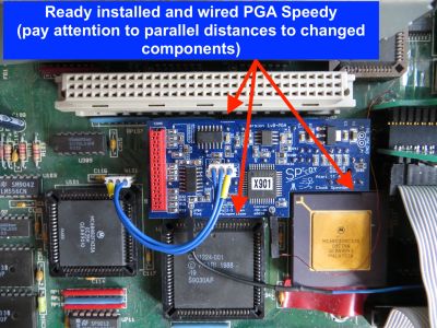
Abb15: PGA TT Mainboard with all changes, ready to install PGA-Speedy
Put Speedy on top of the sockets of U111 up to U116. Please be careful and check that all pins fit correctly into the right socket pins.
Put the small adapter between W101 (mainboard) and W101 (Speedy).
Conversion of a Daughterboard TT
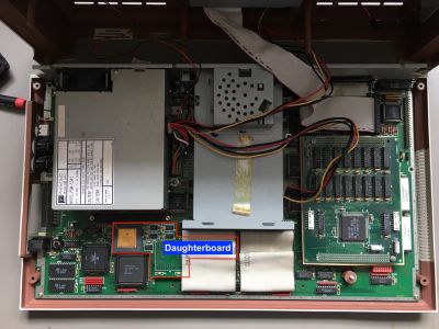
Your TT mainboard looks like the next picture. Remove the old daughterboard, unplug the connector coming from the oscillator and put the old daughterboard to a good place to store them.
Abb16: Mainboard DB TT with marked daughterboard
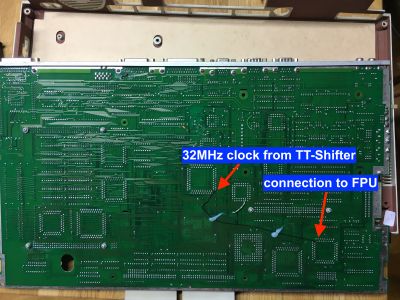
The next step is to build new the signal line for the clock speed from the coprocessor. Atari delivered the first daughterboard TT with fix 16 MHz coprocessor clock speed. The last daughterboard TT fix by Atari themselves under the mainboard to 32 MHz clock speed. Both solution are fixed solution without any jumper! Remember please, that W101 inside of the daughterboard TT has only two instead of three pins like in the other TTs! The next picture show the 32 MHz clock speed patch for the coprocessor.
Abb17a-b: Coprocessor clock patch made by Atari themselves
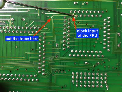
By a fluke the signal clock line of the coprocessor is cut through via Atari. We remove the original black cable between Atari TT Video Shifter and coprocessor and made a new longer cable, connected to the clock pin of the coprocessor. At the other side please solder a female socket pin and connect this socket pin to the back side of DB Speedy.
The next step is, to connect the oscillator plug at the backside of your new DB-Speedy. Please be sure, that the black cable from oscillator pin seven is connect to the “GND”. Plug the DB-Speedy into the CPU socket. Be careful!
Be sure that your changes matched with the next picture.
Abb18: Backside of DB Speedy with clock line to coprocessor and W101 from the oscillator. Both plug at right place under DB Speedy.
Now the view if all works in the DB TT are finished.
Abb.19: Daughterboard TT Mainboard with new Daughterboard-Speedy
Last steps
Connect the power supply and the VGA monitor to the mainboard of your TT and test your mainboard. Please check all details and make the first start of your TT. If the start screen apply, you have finished your conversion job!
Next step is to find out, which clock speed your Co-processor tolerate. At delivery time the Speedy is configured to 32 MHz coprocessor clock speed. Change the Jumper 1 and 2 in right order onto your Speedy to increase or decrease the speed of your coprocessor.
After all reassemble the rest of your TT. All work is done. Gratulations!
2021, July
Best regards
your Thunderstorm Team
Stand: 07.07.2021 Tuxie & R^2
